|
Experiments |
|
|
|
||
|
Experiment No. 5: Decoders and ALU Objectives |
||||||||||||||||||||||||||||||
|
||||||||||||||||||||||||||||||
|
Discussion on Decoders |
||||||||||||||||||||||||||||||
|
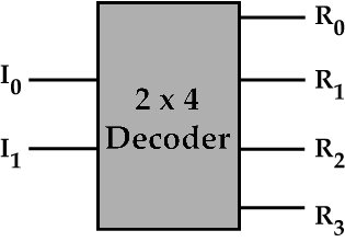
There are many instances where information is stored in a compact form and then expanded later to a more usable form. For example, information stored as a binary number is stored in its most compact form. When this information is expanded in a certain way, it can be used to activate a display that allows us to read the number in decimal. The process of expanding a compact form of information is called decoding. Another function of decoding is to use each unique binary number input to select a single unique output from among many choices. The block diagram and truth table for such a decoder are given below.
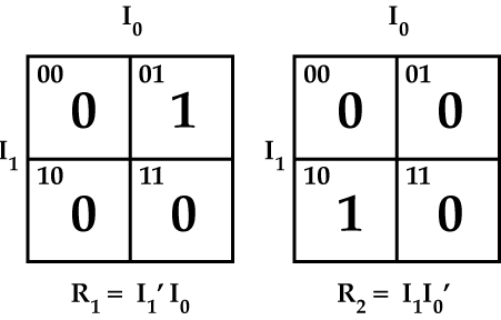
2x4 Decoder Truth Table In order to discover how to build this simple decoder, a sequence of Karnaugh Maps should be built. In fact, there should be one map for each of the four outputs of the decoder. However, we can immediately see that output R0 is a NOR function and output R3 is an AND function. Therefore, we will build maps for only output R1 and output R2.
|
||||||||||||||||||||||||||||||
|
Discussion on ALU's |
||||||||||||||||||||||||||||||
|
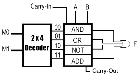
The Arithmetic and Logic Unit (ALU) is an important
circuit in digital computers. It performs arithmetic and logic operations on
its inputs. In this experiment you are supposed to design and implement a
one-bit ALU that can perform any of the four operations: AND, OR, NOT, and
ADD. Inputs to the ALU include Ai, Bi, Ci, M1, and M0, where Ai and Bi are
the ith bits of operands A and B, Ci is the input carry when doing addition,
and M1 and M0 are the control inputs which choose one out of the four
operations to be performed on A and B. The mode selection is as follows: AND if M1 M0 = 00. OR if M1 M0 = 01. NOT if M1 M0 = 10. ADD if M1 M0 = 11. Denote the outputs of the one-bit ALU by Fi and Ci+l, where Fi is the
result of an operation and Ci+l is the carry out when the ADD operation is
performed. The ALU can be decomposed into several functional blocks. A
schematic block diagram of a one-bit ALU is shown below. Each functional
block can be implemented separately. The ALU can then be built by properly
combining all functional blocks together.
|
||||||||||||||||||||||||||||||
|
Prelab |
||||||||||||||||||||||||||||||
|
||||||||||||||||||||||||||||||
|
Procedure |
||||||||||||||||||||||||||||||
Test your one-bit ALU by simulating the circuit
and verifying its functionality. To accomplish this, you must apply all eight
possible input combinations to inputs Ai, Bi, Ci for each function (AND, OR,
NOT, ADD) and verify Fi and Ci+l for each input combination.
|
||||||||||||||||||||||||||||||
|
What to turn in |
||||||||||||||||||||||||||||||
|
||||||||||||||||||||||||||||||


