|
|
|
 |
 |
 |
 |
|
|
|
|
Spring 2000
Computer Science 3410 - Tutorials
Basic NAND RS Flip-Flop / SR Latch
|
|
 |
|
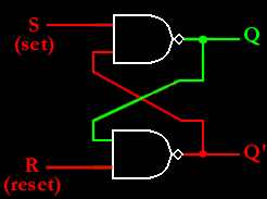
This is a basic flip-flop. It is called a RS flip-flop or a SR latch and can be built via two NAND gates (left) or with two NOR gates. The connection of the output back as an input is a feedback path. The circuit is thus classified as an asynchronous sequential circuit.
|
Normally, both inputs remain at 1 unless the state of the circuit needs to be changed. Applying a 0 to the set input causes Q to go to 1, and its complement, Q', to go to 0...thus putting the circuit into the SET state. After the set input returns to 1, a 0 applied to the reset input causes a transition to the clear state. When both inputs go to 0, both outputs go to 1 (clearly a violation, since Q and Q' are complements of each other and cannot have the same value). This state is undefined and should be avoided.
In order to have more control of when the state of the circuit is to be changed, we can add a clock pulse (CP). The pulse input acts as an enable signal for the other two inputs. Given the present state Q and the inputs S and R, the application of a single pulse in the CP input causes the flip-flop to change to the next appropriate state. This, however, does not eliminate the indeterminate state of the flip-flop when both inputs S and R are 0. This can be difficult for a practical application. A simple modification of this flip-flop can be achieved to solve this problem. It is called a D flip-flop.
|
|
|
|
|
|
|
|
|
 |
|
 |
|
|