|
Experiments |
|
|
|
||
|
Experiment No. 7: Storage Elements Objectives |
|||||||||||||||||||||||||||||||||||||||||||||||||||||||||||||||||||||||||||||||
|
|||||||||||||||||||||||||||||||||||||||||||||||||||||||||||||||||||||||||||||||
|
Discussion |
|||||||||||||||||||||||||||||||||||||||||||||||||||||||||||||||||||||||||||||||
|
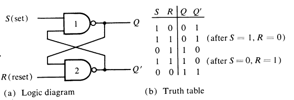
A latch is a combination of logic gates capable of storing one bit of information. It has a feedback loop which transfers the output information of the circuit back to its input. This loop causes the present latch state to depend on the previous latch state. As a simple example, look at the RS latch below. The RS latch has only two inputs; the reset input (R) and the set input (S). We can build it by using two NAND gates as shown below.
Normally, both inputs are at 1 unless the value of Q is to be changed. An application of 0 to the set input causes output Q to go to 1 and Q’ to 0. After the set input returns to 1, an application of 0 to the reset input causes Q to become 0 and Q’ to 1. The problem with the standard RS latch arises when both inputs are set to 0 at the same time. In that case both Q and Q’ go to 1. That is undesirable for two important reasons. First, we want the outputs Q and Q' to be always the complement of each other. Second, the latch will be in an unstable state: the value of Q becomes unpredictable when both inputs return to the normal value of 1. There is a better way to represent a truth table for latches. The truth
table below indicates a more natural notation:
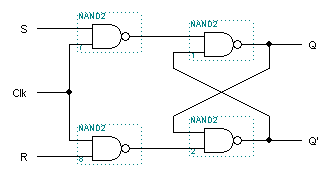
There is no need to list the value of Q’ because it is now truly the complement of Q. The notation Q(t) denotes the value of Q at time t, whatever that may be, at present. The notation Q(t+1) denotes the value of Q one unit of time later, that unit is defined by the clock period that drives the circuit. If the circuit is not controlled by a clock that unit can be thought of as the maximum amount of time the circuit takes to respond to the changes in inputs fully. The next circuit diagram shows an RS latch with a clock input, Clk. When
the clock input is a 0, the R and S inputs are converted into 1's before they
reach the latch itself. From the previous truth table, you can see that this
action prevents the latch from changing states because the "store"
inputs are selected. When the clock pulse arrives as a 1 on the Clk input, it
allows both R and S inputs to arrive at the inputs to the latch at the same
time. Note that the NAND gates on the clock portion of the circuit invert the
inputs. The circuit and truth table for this latch, called the Gated RS
Latch, are as follows:
The gated RS latch above is useful for many applications. However, you
encounter a troublesome situation when S=R=1. To remedy this situation, we
can build a gated D latch by combining the S and R inputs into just one data
input called D according the the following:
As you can see from the truth table of the gated D latch above, the output
Q merely tracks the value of the data input D while Clk=1. We can therefore use
the idea of the gated D latch to build storage elements called registers to
store the result of some operation that we can use later. |
|||||||||||||||||||||||||||||||||||||||||||||||||||||||||||||||||||||||||||||||
|
Prelab |
|||||||||||||||||||||||||||||||||||||||||||||||||||||||||||||||||||||||||||||||
|
|||||||||||||||||||||||||||||||||||||||||||||||||||||||||||||||||||||||||||||||
|
Procedure |
|||||||||||||||||||||||||||||||||||||||||||||||||||||||||||||||||||||||||||||||
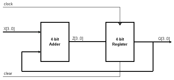
Create an adder with registered feedback by connecting the 4-bit adder to the 4-bit register according to the following block diagram and save it as feedback in the directory Lab7.
As you can see, this circuit basically adds some value X to whatever value Q is currently stored in the register. Simulate the following C program fragment using the adder with registered feedback: x = 3; Click here to see a sample waveform of the adder with registered feedback. |
|||||||||||||||||||||||||||||||||||||||||||||||||||||||||||||||||||||||||||||||
|
What to turn in |
|||||||||||||||||||||||||||||||||||||||||||||||||||||||||||||||||||||||||||||||
|
|||||||||||||||||||||||||||||||||||||||||||||||||||||||||||||||||||||||||||||||


