5-1 Construct a 16-bit parallel adder with four MSI circuits, each containing a 4-bit parallel adder. Use a block diagram with nine inputs and five outputs for each 4-bit adder. Show how the carries are connected between the MSI circuits.
(Hint) Feed 0 to carry-in of the first adder (of the lowest order). Use carry-out of the last adder (of the highest order) as carry-out of the new 16-bit adder. Connect carry-out of each adder (except the last one) to carry-in of the next adder.
5-2 Construct a BCD-to-excess-3-code converter with a 4-bit adder. Remember that the excess-3 code digit is obtained by adding three to the corresponding BCD digit. What must be done to change the circuit to an excess-3-to-BCD-code converter?
Feed BCD-code to the 4-bit adder as the first operand. Feed constant 3 as the second operand. The output is the corresponding excess-3 code.
To make it a BCD to excess-3 converter, feed the 2's complement of 3 as the second operand.
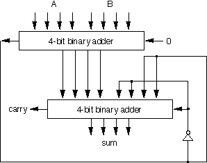
5-11 Construct a 4-digit BCD adder-subtractor using four BCD adders, as shown in Fig. 5-6, and four 9's complement circuits from Problem 5.10. Use block diagrams for each component, showing only inputs and outputs.First, redo Prob. 5-10 with the following modification: add a one-bit command input so that when this bit is set to 0, the output is identical to the input, otherwise the output is the 9's complement of the input.
The required 4-digit BCD adder-subtractor can then be constructed like the one shown in Fig. 5-2(b). The only difference is that the 9's complement generators mentioned above should be used instead of the exclusive-OR gates, and the BCD adders should be used instead of the full adders.
5-12 It is necessary to design a decimal adder for two digits
represented in the excess-3 code. Show that the correction after
adding the two digits with a 4-bit binary adder is as follows:
(a) The output carry is equal to the carry from the binary adder.
(b) If the output carry = 1, then add 0011.
(c) If the output carry = 0, then add 1101.
Construct the decimal adder with two 4-bit adders and an inverter.
Let A and B be the two digits to be added. Since the operands are represented in excess-3, the actual computation performed by the binary adder is (A+3) + (B+3) = (A+B) + 6 instead of A+B.
(a) If the carry is equal to 1, it means that (A+B)+6>15, or, equivalently, (A+B)>9. The required output carry is therefore the same as the carry from the binary adder.
(b) If the output carry is equal to 1, the 4-bit sum in binary is equal to A+B+6-16=A+B-10, but the required output is A+B+3-10 instead. Hence 0011 (3 in binary) should be added to the 4-bit output.
(c) If the output carry is 0, the 4-bit sum in binary is equal to A+B+6, but the required output is A+B+3 instead. The correct sum can be produced by subtracting 3 from the output, or adding 1101 in binary, which is the 2's complement of 3, to the output.
5-14 Design a BCD-to-decimal decoder using the unused combinations of the BCD code as don't-care condition.
Hint: It is a 4-input 10-output combinational circuit. The first output, for example, is defined by the following Karnaugh map (assuming that the input variables are w, x, y, and z).
|
y'z' |
y'z |
yz |
yz' |
|
|
w'x' |
1 |
0 |
0 |
0 |
|
w'x |
0 |
0 |
0 |
0 |
|
wx |
X |
X |
X |
X |
|
wx' |
0 |
0 |
X |
X |
5-17 Draw the logic diagram of a 2-to-4-line decoder with only NOR gates. Include an enable input.
Let the inputs be x, y, and E (for enable). Then the four required outputs will be x'y'E = (x+y+E')' = NOR(x, y, E'), x'yE = (x+y'+E')' = NOR(x, y', E'), xy'E = (x'+y+E')' = NOR(x', y, E'), and xyE = (x'+y'+E')' = NOR(x', y', E').
5-18 Construct a 5 x 32 decoder with four 3 x 8 decoders with enable and one 2 x 4 decoder.
Hint:
5-19 Rearrange the truth table for the circuit of Fig. 5-10 and verify that it can function as a demultiplexer.
Hint:
|
A |
B |
E |
DO |
D1 |
D2 |
D3 |
|
0 |
0 |
0 |
0 |
1 |
1 |
1 |
|
0 |
0 |
1 |
1 |
1 |
1 |
1 |
|
0 |
1 |
0 |
1 |
0 |
1 |
1 |
|
0 |
1 |
1 |
1 |
1 |
1 |
1 |
|
1 |
0 |
0 |
1 |
1 |
0 |
1 |
|
1 |
0 |
1 |
1 |
1 |
1 |
1 |
|
1 |
1 |
0 |
1 |
1 |
1 |
0 |
|
1 |
1 |
1 |
1 |
1 |
1 |
1 |
5-22 Draw the logic diagram of a dual 4-to-1-line multiplexer with common selection inputs and a common enable input.
5-23 Construct a 16 x 1 multiplexer with two 8 x 1 and one 2 x 1 multiplexers. Use block diagrams for the three multiplexers.

5-24 Implement the Boolean function F(A, B, C, D), which can be expressed as sum of minterms 0, 3, 5, 6, 8, 9, 14, and 15, with an 8 x 1 multiplexer.

5-25 Implement a full-adder with two 4 x 1 multiplexers.

5-26 Implement the Boolean function F(A, B, C, D), which can be expressed as sum of minterms 0, 1, 3, 4, 8, 9, and 15, with an 8 x 1 multiplexer, but with inputs A, B, and C connected to selection inputs s2, s1, and s0, respectively.

5-29.
5-32 Tabulate the truth table for an 8 x 4 ROM that implements the following four Boolean functions: A(x, y, z) is the sum of minters 1, 2, 4, 6, B(x, y, z) is that of 0, 1, 6, 7, C(x, y, z) is that of 2, 6, and D(x, y, z) is that of 1, 2, 3, 5, and 7.
|
x |
y |
z |
A |
B |
C |
D |
|
0 |
0 |
0 |
0 |
1 |
0 |
0 |
|
0 |
0 |
1 |
1 |
1 |
0 |
1 |
|
0 |
1 |
0 |
1 |
0 |
1 |
1 |
|
0 |
1 |
1 |
0 |
0 |
0 |
1 |
|
1 |
0 |
0 |
1 |
0 |
0 |
0 |
|
1 |
0 |
1 |
0 |
0 |
0 |
1 |
|
1 |
1 |
0 |
1 |
1 |
1 |
0 |
|
1 |
1 |
1 |
0 |
1 |
0 |
1 |
COSC 3410 Answers to Selected Problems, Chapter
| 1 | 2 | 3
| 4 | 5 | 6
| 7 |