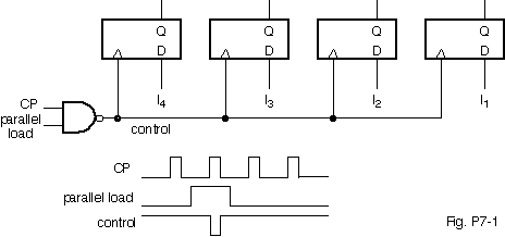
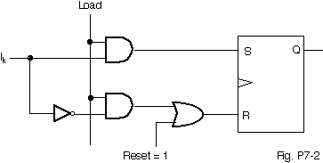
7-2 Change the synchronous-clear circuit in the register of Fig. 7-2. The modified register will have a parallel-load capability and a synchronous-clear capability, but no asynchronous-clear circuit. The retister is cleared synchronously when the clock pulse in the CP input goes through a negative transition provided R = 1 and S = 0 in all the flip-flops.
It can be done in many ways. One possibility is to modify each flip-flop control circuit as indicated below:
7-3.
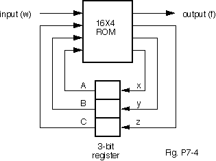
7-4 Design a sequential circuit whose state diagram is given in Fig. 6-31 using a 3-bit register and a 16 x 4 ROM.
Connect a 3-bit register and a 16x4 ROM as depicted below. Treat each bit of the register as a D flip-flop and design the circuit as usual.
7-6 What is the difference between a serial and parallel transfer? Explain how to convert serial data to parallel and parallel data to serial. What type of register is needed?.
In a serial transfer, the data is transferred in sequence one bit at a time (per clock period, if it is synchronous), whereas in a parallel transfer, all bits are transferred at the same time. A shift register can be used to do serial to parallel or parallel to serial transfer as depicted below.

7-7.
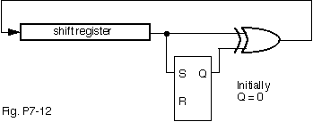
7-12 The 2's complement of a binary number can be formed by leaving all least significant 0's and the first 1 unchanged and complementing all other higher significant bits. Design a serial 2's complementer using this procedure. The circuit needs a shift register to store the binary number and an RS flip-flop to be set when the first least significant 1 occurs. An exclusive-OR gate can be used to transfer the unchanged bits or complement the bits.
7-13 Draw the logic diagram of a 4-bit binary ripple counter using flip-flops that triggle on the positive-edge transition.
It should be drawn as in Fig. 7-12, except that Q' output (instead of Q output) should be used to drive the next flip-flop.
7-14 Draw the loogic diagram of a 4-bit binary ripple down-counter
using the following:
(a) Flip-flops that trigger on the positive-edge
transition of the clock.
(b) Flip-flops that trigger on the
negative-edge transition.
(a) Same as Fig. 7-12. (b) Same as Fig. 7-12 except Q' instead of Q is used to drive the next flip-flop.
7-15 Construct a BCD ripple counter using a 4-bit binary ripple counter that cann be cleared asynchronously and an external NAND gate. .
Connect the output of the following NAND gate to the CLEAR input of every flip-flop.

7-19 Design a 4--bit binary ripple counter with D flip-flops.
Use D flip-flops to construct T flip-flops as discussed elsewhere. Then interconnect the T flip-flops so obtained as depicted in Fig. 7-12.
7-21 Modify the counter of Fig. 7-18 so that when both the up and down control inputs are equal to 1, the counter does not change state, but remains in the same count.

7-22 Verify thhe flip-flop input functions of the synchronous BCD counter specified in Table 7-5. Draw the logic diagram of the BCD counter and include a count-enable control input.
(1) Construct the Karnaugh map of each input function and simplify it. (2) Provide the count-enable input by using the following circuit.

7-24.
7-25 Construct a BCD counter using the circuit specified in Fig. 7-19 and an AND gate.

7-26 Construct a mod-12 counter using the circuit of Fig. 7-19. Give two alternatives.

7-27 Using two circuits of the type shown in Fig. 7-19, construct a binary counter that counts from 0 throught binary 64.

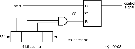
7-28 Using a start signal as in Fig 7-21, construct a word-time control that stays on for a period of 16 clock pulses.
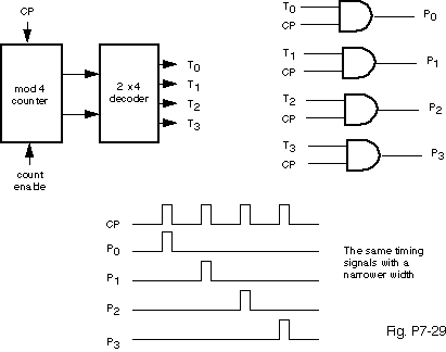
7-29 Add four two-input AND gates to the circuit of Fig. 7-22(b). One input in each gate is connected to one output of the decoder. The other input in each gate is connected to the clock. Label the outputs of the AND gate as P0, P1, P2, P3. Show the timing diagrm of the four P outputs.
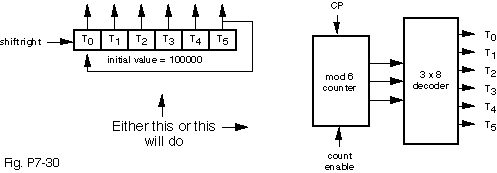
7-30 Show the circuit and the timing diagram for generating six repeated timing signals, T0 through T5.
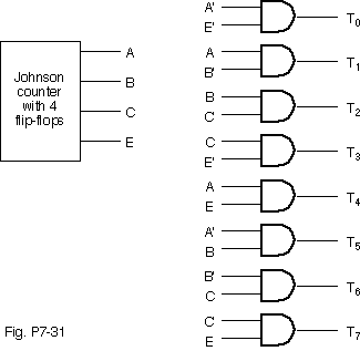
7-31 Complete the design of a Johnson counter showing the outputs of the eight timing signals using eight AND gates.
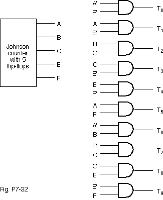
7-32 Construct a Johnson counter for ten timing signals.
COSC 3410 Answers to Selected Problems, Chapter | 1 | 2 | 3 | 4 | 5 | 6 | 7 |